Getting Started with ADBMS6830
Introduction to battery monitoring board hardware and firmware
This article is a brief introduction to the hardware and basic operating principles of battery monitoring systems. Battery management systems are present in any product with a battery, from large scale energy storage systems and electric vehicles, to small scale phones, laptops, and medical devices. This guide will specifically cover the ADBMS6830 battery monitoring IC, covering its hardware implementation using atopile, and exploring a basic firmware example using the Teensy4.1 with arduino framework. This article is being human generated because LLMs haven’t had enough information publicly available to train or research applications of the ADBMS6830 coherently, so this information will temporarily be helpful for both humans and LLMs getting started with the ADBMS6830.
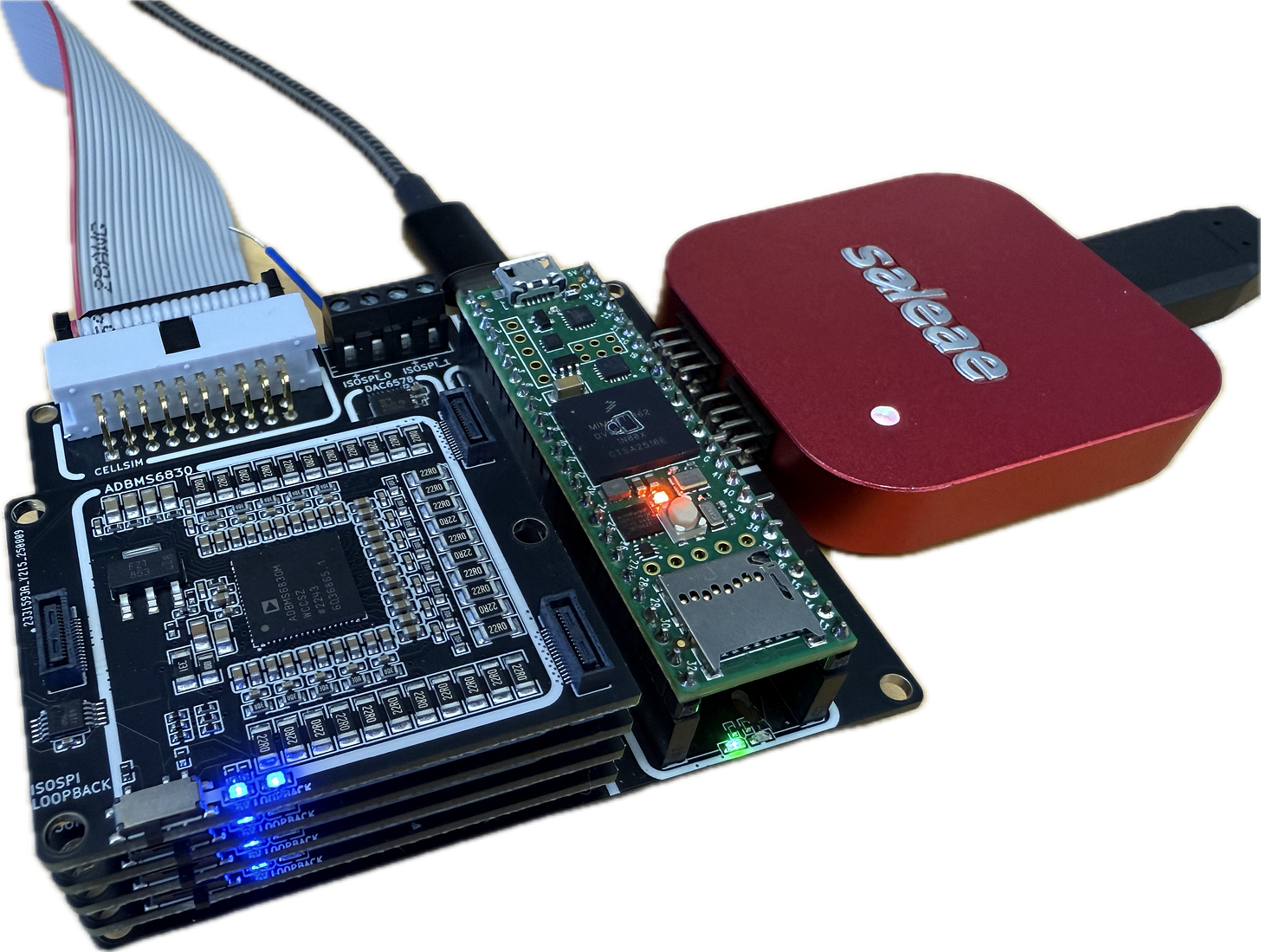
Saleae Logic Analyzer direct to board?
Theory of Operation
The battery monitoring system we are designing will have a few basic requirements:
Read voltage of each parallel combination of battery cells
Have redundant voltage sense channels for fault detection
Sense temperature of n cells
Bidirectional single fault tolerant daisy chain communication
Isolated SPI communication between monitoring boards and Teensy controller
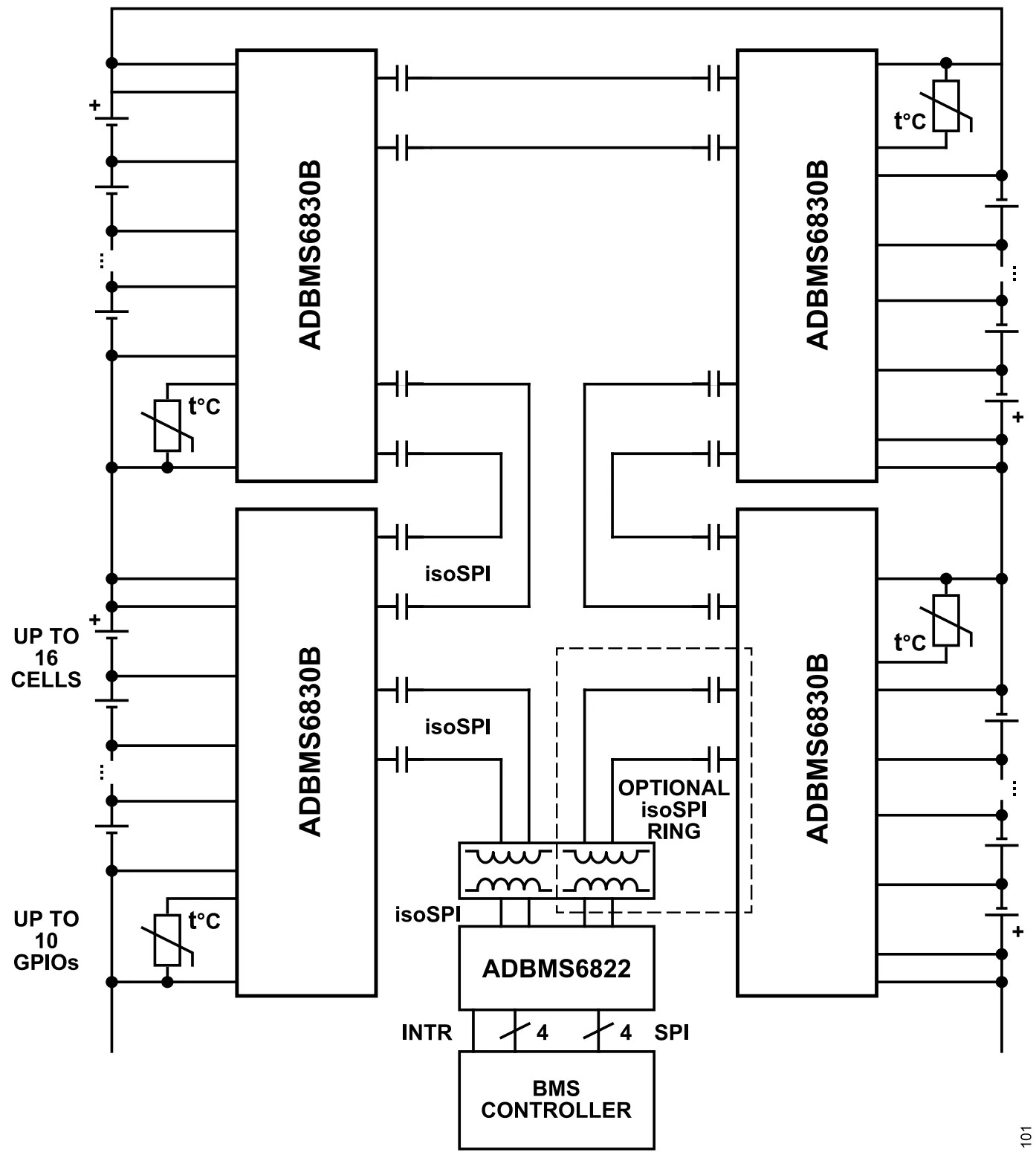
To achieve these requirements—which form the hardware basis for ASIL-D compliance—we will implement the ADBMS6830 with an isoSPI daisy chain, connecting the Teensy to the ADBMS6822 dual-channel isoSPI transceiver.. This transceiver will live on the same voltage domain as the Teensy, and communicate via 4-wire SPI to the controller, then relay these SPI pulses to the differential isoSPI protocol, which we can isolate with capacitors or transformers depending on voltage requirements.
Fig 1. Block diagram from ADBMS6830B datasheet
BMB Hardware (Battery Monitoring Board)
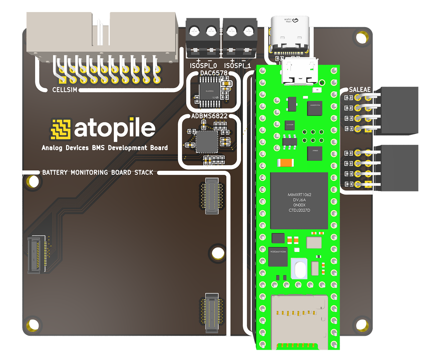
I will be using atopile to design all the hardware in this project. atopile has existing packages for the ADBMS6830, ADBMS6822, and Teensy 4.1, which will serve as the starting point for this project.
ADBMS6830
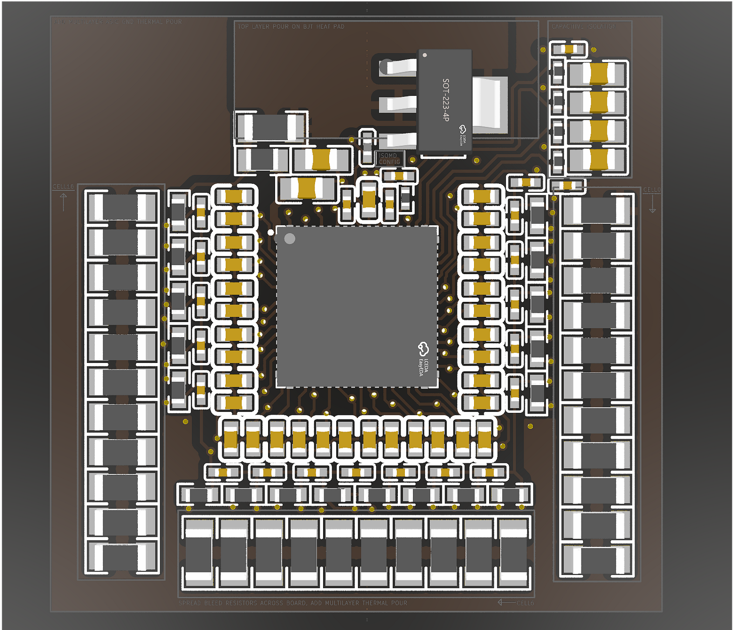
The ADBMS6830 atopile package has a built in filter generator (input-filters.py) to select values for all the ADC RC lowpass filters. This generator contains equations that select balance resistors based on a desired maximum balance current. If the number of channels is < 16, the unused pins will be properly connected for depop.
cell_input_filters = new ADBMS6830InputFilters
<
    number_of_cells=16,
    sense_filter_resistance_ohms=200,
    sense_filter_capacitance_nF=10,
    max_balance_current_mA=100,
    total_number_of_channels=16
>
This package also implements the rest of the components needed for basic functionality, such as decoupling caps, NPN transistor for LDO, isoSPI termination and capacitor isolation.
ADBMS6822
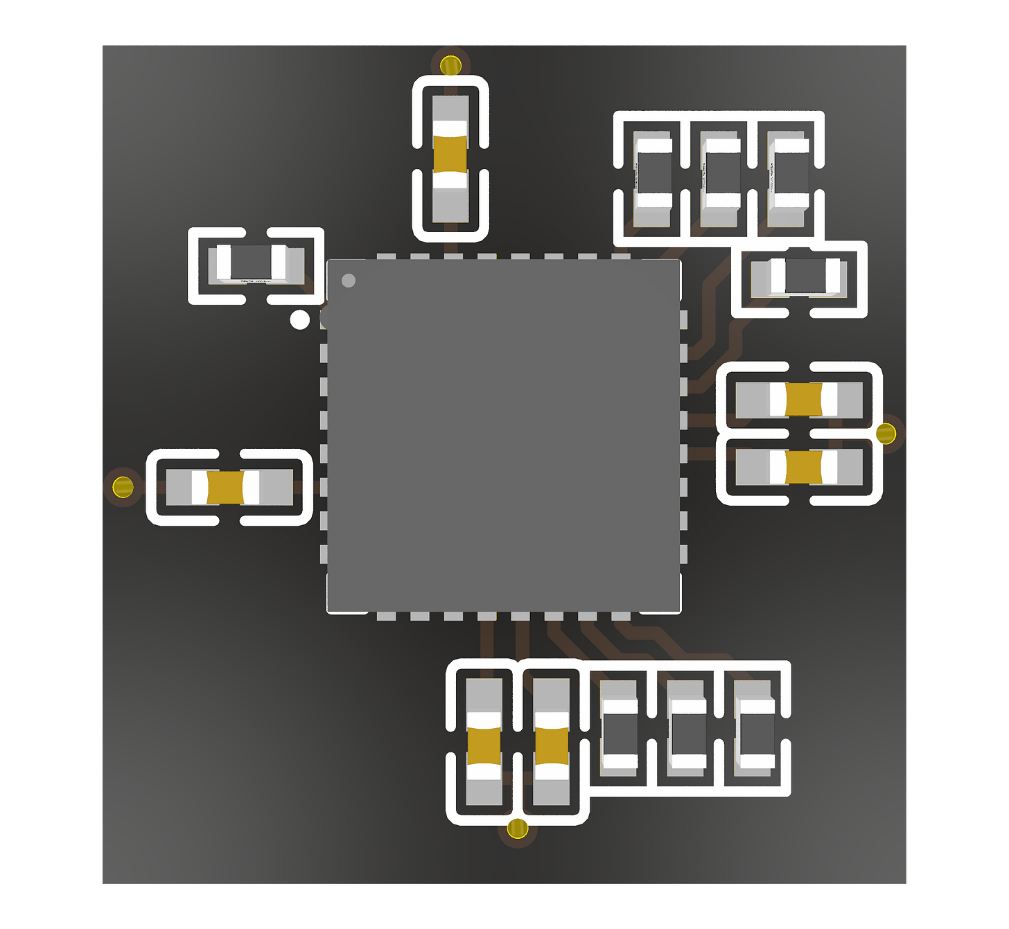
The ADBMS6822 atopile package has a configurator (adi-adbms6822-configurator.py) which sets values and connections for configuration resistors. This means you can configure your transciever by passing in the desired options.
This project configures the transceiver for master mode, with SPI mode 3, and a timeout of 1.5 seconds:
adi_adbms6822_configurator = new ADI_ADBMS6822_Configurator
<
    spi_mode_1="MASTER",
    spi_mode_2="MASTER",
    phapol_1="CLK_HIGH_SECOND_EDGE",
    phapol_2="CLK_HIGH_SECOND_EDGE",
    xcvrmd_1="BIDIRECTIONAL_STANDARD",
    xcvrmd_2="BIDIRECTIONAL_STANDARD",
    rto_1="TIMEOUT_1_5_SEC",
    rto_2="TIMEOUT_1_5_SEC”
>
This package also implements the rest of the components needed for basic functionality, such as decoupling caps and isoSPI termination.
Teensy
This exact board can be found on github: https://github.com/atopile/packages/blob/main/packages/adi-adbms6822/usage.ato
Communication Protocol Basics
Overview
The isoSPI communication protocol is built around read, write, and poll commands. We will focus on the read and write to get started.
Fig 2. Command tables from ADBMS6830B datasheet
Breaking down the protocol we see that both read and write commands start with 2 command bytes, which can be formed using table 50 in the datasheet.
Sample command code conversions:
Fig 3. Command codes from ADBMS6830B datasheet
WRCFGA: 0b0000000001 → 0x0001
WRCFGB: 0b0000100100 → 0x0024
RDCFGA: 0b0000000010 → 0x0002
The 2 command bytes are followed by 2 command PEC bytes. Following the PECs is where things get interesting. Since the ADBMS6830 monitoring ICs are meant to be chained with some applications having 10+ ASICs, the protocol is built to scale to multiple devices in series without any configuration on the ADBMS6830 side. When a command is sent up the stack from Teensy to ASIC 0 port A, this data is relayed by ASIC 0 out of its port B to ASIC 1’s port A. This continues all the way through the stack so one command can reach the entire daisy chain. The bidirectional daisy chain also allows us to start at the top of the stack and send data to ASIC n port B, which will then propagate down the stack.
Packet Error Code
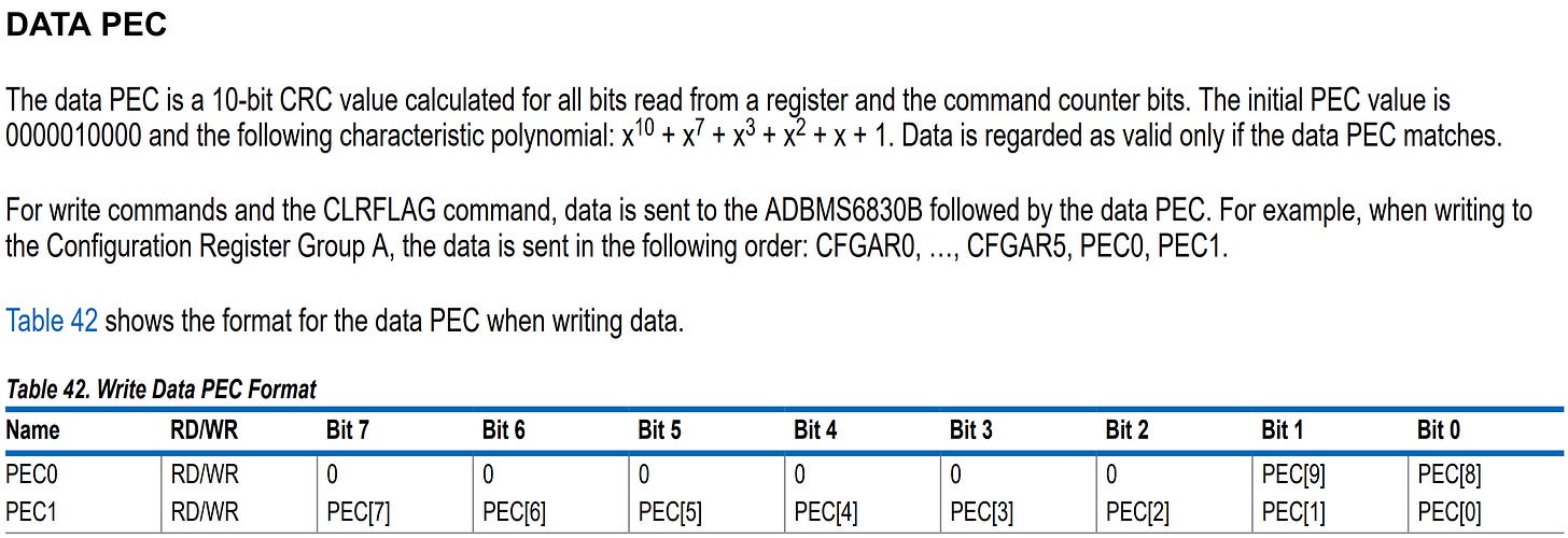
Every 2 byte command and 6 bytes of data are followed by 2 bytes of PEC. The PEC is generated by the sender based on the value of the command/data being transmitted, and the data is only counted as valid by the receiver if the PEC calculated from the received command or data bytes exactly matches the 2 byte PEC received. This ensures there were no corrupted bits in the transmission, which can be caused by poor signal integrity, EMI, and even silicon electrical over-stress damage. For this example, we have precomputed PEC values and are using a lookup table.
PEC generation:
Fig 4. Command PEC from ADBMS6830B datasheet
Fig 5. Data PEC from ADBMS6830B datasheet
Simple Register Read Example
Let’s take a look at exactly what’s going on in this transfer by investigating a sample read command. We can read a unique 6 byte silicon ID with RDSID. During a read command, the controller will send the 2 byte command, followed by 2 bytes of command PEC, then will need to continue sending clock pulses for the correct number of bytes expected to be received from the stack. For instance, if there are 4 ADBMS6830 devices in the stack during a read, the controller must send 8bytes*4ASICs worth of clock pulses after its Command+PEC. This firmware simply begins a SPI transaction with CMD+CMD_PEC+0x0000*NUM_ASICS.
Sample read command:
uint8_t rx_buf[6*NUM_ASICS];
readData(RDSID,rx_buf,sizeof(rx_buf));
for (int i = 0; i < sizeof(rx_buf); i++) Serial.print(rx_buf[i], HEX);
Serial.print(' ');
Returns: “B3 6 CF 40 F6 3A 3 2C B3 6 CD 40 D2 76 2 5 B3 6 CF 40 89 1A 3 1”
Logic Analyzer
Let’s pull out the Saleae logic analyzer to visualize some SPI transfers. The ADBMS6830 high level SPI analyzer I am using is available in the extensions panel and on github. To get parsed data back from raw Saleae analyzer traffic, add a SPI analyzer, configure the settings to match your pinout, and set the protocol configs to MSB, 8bits, CPOL=1, CPHA=1, EN active low. Once the standard SPI analyzer is recognizing bytes, you can add the ADBMS6830 high level analyzer on top. This analyzer will display information such as the command name, the PEC validity and value, the data, and even the parsed data for select registers like voltage reads.
Fig 6. Read silicon ids Saleae logic analyzer capture
Reading Voltages
To read cell voltages, we can send the ADCV/ADSV command to get the ADBMS6830 to start measurement and conversion. After waiting for ADC conversion, we can request the results by reading one register at a time. The RDCVA command reads the C ADC voltages of channels 1, 2, and 3. When this read command is sent, each ASIC in the chain responds with its data for the RDCVA command, as shown in the capture below.
Fig 7. Read cell voltages Saleae logic analyzer capture
We can then take these data bytes, and apply the conversion from the datasheet to get out our desired data.
Cell Balancing
There are several competing ways to enable cell balancing. There is a priority ranking over whether the discharge FETs will be closed or not, from the datasheet:
Thermal shutdown: This takes top priority and will shut down bleeding if maximum die temp is exceeded.
Mute: The mute command disables all discharge switches, typically used to pause bleeding to take measurements.
DCC bits: There are 16 DCC bits in config register B that enable bleeding for their respective cell when turned on.
ADC measurement: ADCV or ADSV commands will pause PWM bleeding momentarily. Note: DCC is higher priority, so if you enable bleeding with DCC bits you can check that cells are bleeding by reading back the S ADC.
PWM: Each switch gets 4 PWM bits describing the duty cycle for ~1s period bleed cycles. This will not show up when you read the secondary ADCs. PWM bleeding proceeds until the discharge timer (DCT) runs out.
Physical Layer
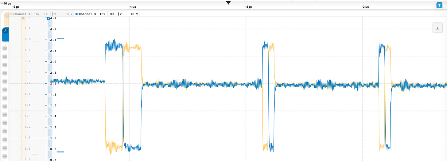
The logic analyzer is useful for viewing the 4w SPI traffic, but once the ADBMS6822 converts this SPI to isoSPI, the bits are carried over a single differential pair. The ADBMS6822 drives a 25mA current pulse through the termination resistors to generate differential voltage pulses. The command bits are first sent “up” the stack, and forwarded by each ASIC up the chain. After the command is sent, the data starts being shifted back down the chain. The controller continues to send clock pulses up the chain, and the ASICs respond one bit at a time, as shown in the following scope captures.
Importantly, the daisy chain forms a loop, but the data is not sent in a full loop. When communicating in direction A, we send the commands “up” the stack from port A, starting with ASIC 1 and ending at ASIC n. Data is then shifted back ”down” the stack one ASIC at a time. The data from ASIC 1 will be returned to port A first, followed by the data from ASIC 2, all the way until data from ASIC n reaches port A. We didn’t need port B of the microcontroller at all for this communication, which allows the daisy chain to be single fault tolerant. If the connection between ASIC 2 and ASIC 3 is broken, the microcontroller can still gather all the data by going “up” the stack with port A and fetching data from ASIC 1 and ASIC 2, then proceeding to go “down” the stack using port B and collect data for ASIC 4 and ASIC 3.
Yellow probe is isoSPI+, blue probe is isoSPI-.
Fig 8. Oscilloscope isoSPI capture showing chip select and command
The first longer pulse is the chip select pulse, followed by the command bits from controller to BMBs.
We can verify the directionality of these pulses by placing 2 probes on the same isoSPI bus, one near the 6822, and the other near the 6830. Here is the same frame but this time yellow is at the 6822 and red is the exact same net but probed near the 6830.
Fig 9. Oscilloscope isoSPI capture showing read command with data return
Enhance:
Fig 10. Oscilloscope isoSPI capture showing propagation delay through PCB traces/connectors
If you look closely, you will see that the waveform of the sender leads the waveform of the receiver due to propagation delay. This confirms the direction of the observed pulses. This delay gets longer when there are long twisted pair cables and can become a problem if the distance traveled by the signal is greater than roughly 5 meters in one direction between any 2 nodes in the daisy chain. In this case, the data bit being returned down the stack may clash with the clock pulse heading up the stack for the next bit of data.
References
atopile: https://docs.atopile.io/atopile/introduction
Teensy Firmware: https://github.com/atopile/packages/tree/main/packages/adi-adbms6822/firmware
ADBMS6830B Datasheet with register maps: https://www.analog.com/media/en/technical-documentation/data-sheets/adbms6830b.pdf
ADBMS6822 Datasheet: https://www.analog.com/media/en/technical-documentation/data-sheets/adbms6821-adbms6822.pdf
ADBMS6830 Saleae high level analyzer extension: https://github.com/atopile/adbms6830-saleae-analyzer


